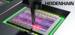
ASMPT ALSI is the inventor of multi-beam laser dicing and grooving. The multi laser beam dicing and grooving process is the technology with very low thermal impact while having a very high productivity. ASMPT ALSI’s solutions enable you to reduce your manufacturing cost significantly and to execute your semiconductor technology road map.
Technology
To enable the low cost of ownership all modules within the system support and contribute to achieve this proposition. To keep up with the demanding semiconductor market, continuous technology development enables; smaller, better and more cost effective products for wafer dicing and grooving applications.
Products
We offer laser dicing and grooving systems that enable the lowest cost of ownership through the shortest process time and high flexibility. This ensures that ASMPT ALSI’s laser systems are ideally suited for your application.
Application
We develop laser dicing and grooving solutions that enable semiconductor manufacturers to reduce the product manufacturing cost through yield improvement, higher productivity, and increased number of dies per wafer. Our expertise is in RFIC, LED, IC, Low-K and Discrete.
ASMPT the leading global provider of hardware and software solutions for the manufacture of semiconductors and electronics, has reached another milestone in its long and successful history. The company has aligned all its segments, business units and regions worldwide under one brand, ‘ASMPT’. Watch the video
The two main requirements for any separation process are a superior cutting quality – in terms of visual appearance and structural integrity of the cut – and a low throughput time. The latter depends to a great extend on the dicing speed thus the material removal rate of the process. In the case of laser dicing both requirements are generally speaking diametrical opposed to each other. The material removal rate scales with increasing laser power, the dicing quality deteriorates accordingly. Typically a fast laser separation process comes along with a wide cut, rough edges, increased volumes of recast and burr as well as a pronounced heat affected zone (HAZ). Read more and watch the video
Last week ALSI shipped the first high power ultra-short pulse LASER1205 grooving system to a customer with a leading position in the display industry. By the application of new technology and close customer collaboration new frontiers are defined for minimal burr height, higher die strength and cost effective UPH for laser grooving applications.
The two main requirements for any separation process are a superior cutting quality – in terms of visual appearance and structural integrity of the cut – and a low throughput time. The latter depends to a great extend on the dicing speed thus the material removal rate of the process. In the case of laser dicing both requirements are generally speaking diametrical opposed to each other. Read more
As in all precision machines, the accelerating mass of the stage introduces deformation and vibrations in the frames, negatively influencing attainable accuracy. This effect is counteracted by an active mount system: linear motors generate counter forces in the frame that will keep vibration on a minimal level. These counter forces are both feed forward signals from the stage motions, and feed back signals to suppress disturbances introduced by the facility floor. Watch the video
Multi beam Matrix laser grooving process allows full removal (grooving) of the top layers (Low-K, Metals and passivation, etc). The multi beam matrix grooving process creates a U-Shape groove profile with consistent industry standard quality (low burr, no chipping, smooth groove profile). The unique slider concept (wafer stepper concept) allows high accuracy and reproducibility. Together with unique and patented “kerf check on the fly” the customer has continuous process control. Read more
ASMPT is the inventor of multi beam semiconductor dicing. With more than 20 years of multi beam laser process experience in high volume manufacturing many billions of parts have been processed. Utilizing the strength of the multi beam process, low power per beam but using many beam to allow high material removal rate with a small (<3um) heat affected zone. The unique slider concept (wafer stepper concept) allows high accuracy and reproducibility. The IR multi beam laser process has proven its value in semiconductor wafer singulations and enabled the ongoing trend of thinner (more fragile) devices and shrinking the dicing street resulting in more die per wafer. Key Features
ASMPT has developed a proprietary process with a unique V-DOE Multi beam process for dicing of thin silicon (<<100 µm) wafers with a low CoO while achieving a high die strength (typically >500 MPa). Read more
The design of ALSI machine platform has been made with productive and accurate laser dicing of semiconductor wafers in mind. It incorporates over 12 years of experience in laser dicing of wafers originally at NXP (formerly Philips Semiconductor), and the extensive know-how available in the well-established semiconductor equipment manufacturers in The Netherlands and Germany. Read more
ASMPT has recently received multiple orders from the leading semiconductor manufacturers in ASIA for their latest generation of encapsulation solution for large format packaging, ORCAS EP Dual Press.
ASM Pacific Technology Limited (“ASMPT”) announced today that its focus on customer excellence has once again been recognised in the VLSIresearch’s annual Customer Satisfaction Survey on Chip Making Equipment. For the past few years, customers have ranked ASMPT among the top 10 BEST equipment suppliers. Read more
ASM Pacific Technology Limited (ASMPT) received the prestigious 2015 Supplier Excellence Award (SEA) from it customer, Texas Instruments (TI). ASMPT was recognised for its outstanding performance as a supplier of lead frames.
In developing a solution that is truly making a difference in semiconductor manufacturing, ASM Pacific Technology Limited (“ASMPT”), a world leader in the supply of semiconductor assembly and packaging equipment and materials as well as surface mount technology solutions, received the 2015 Technology Achievement Grand Award for its Thermo-Compression Bonding (TCB) tool.
ASM Pacific Technology Limited (“ASMPT”) and Siliconware Precision Industries Co., Ltd. (“SPIL”)announced today that both companies will enter into an agreement to establish a joint investment entity to develop and manufacture molded interconnect substrates (“MIS”) to meet the industry’s demand for advanced semiconductor chips with greater functionality.
ASM Pacific Technology is ranked as the no. 1 top assembly equipment supplier in 2014 and earns the coveted “10 best focused suppliers of chip making equipment” in 2015 as well as “the best suppliers of 2015” award once again.