Automation Doesn’t Replace Precision. It Makes Precision Scalable.

For decades, the photonics industry has pushed the boundaries of precision. Nanometer positioning, sub-micron alignment and exceptional optical performance have enabled technologies that were once thought impossible. But achieving precision once is no longer enough. Read more [Picture source: Sander Slagter on linkedin.com]
The Next Competitive Advantage in Photonics Isn’t Precision. It’s Repeatability

Photonics has achieved remarkable levels of precision.Nanometer positioning. Sub-micron alignment. Extraordinary optical performance.But as the industry moves beyond R&D and into high-volume manufacturing, precision alone is no longer enough. Read more [Picture source: Sander Slagter on linkedin.com]
Fast Steering Mirror Solutions for Acquisition, Tracking, and Disturbance Compensation under Dynamic Conditions
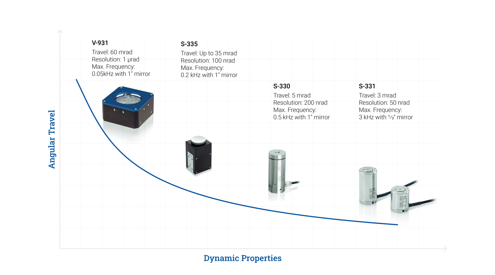
Free-space optical communication (FSOC) enables high-data-rate intersatellite links in low Earth orbit (LEO) constellations. Achieving stable optical connections under dynamic orbital conditions requires highly precise beam control. A recent development project required a space-qualified fast steering mirror for use in FSO terminals that would also be suitable for high-volume production. The goal was to ensure reliable…
The Next Bottleneck in Photonics Isn’t Innovation. It’s Manufacturing
Photonics is accelerating at an unprecedented pace. Silicon photonics, quantum technologies, optical communications, sensing, healthcare — the breakthroughs keep coming. But as the industry shifts from R&D to industrial-scale production, a new reality emerges: The limiting factor is no longer what we can…
Miniature Linear Stages
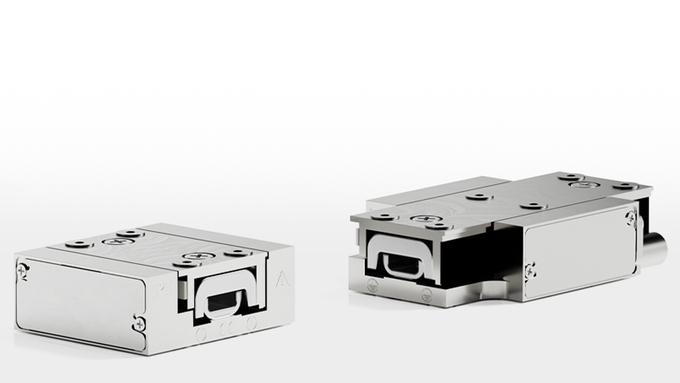
Miniature stages are essential in positioning tasks where available space is limited. Piezomotor solutions like Q-motion®, PIline® and PiezoWalk® allow for the most compact stages due to their direct drive principle. PI’s stages with electromagnetic motors are present and proven in automation tasks worldwide. Ask for your customization! Read more
HOERBIGER Completes Acquisition of PI: Dr. Michael Albiez Appointed New CEO

HOERBIGER successfully completed the acquisition of Physik Instrumente (PI). All regulatory approvals were obtained, and the transaction was concluded as of March 31, 2026. Upon closing, Dr. Michael Albiez was appointed as the new CEO of PI. He succeeds former CEO Markus Spanner, who is no longer with the company. Read more
Quantum technology is evolving rapidly — and so are the demands for precision

Cryogenic 6-axis hexapods play a key role in enabling reliable, ultra-precise optical alignment under extreme conditions. Read more [Picture source: Sander Slagter on linkedin.com]
Miniature Stages
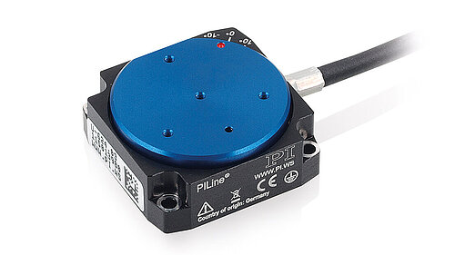
Miniaturized stages and manipulators are essential in applications, where space is limited. This includes mobile applications for measuring and medical devices, in industrial microassembly or use for research, e.g. in UHV and non-magnetic environments. Read more
Simultaneous Electronic Photonic Wafer-Level Testing with a Scalable Technology Platform
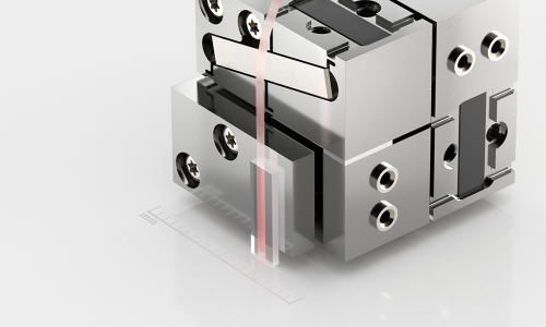
Next-generation devices require wafer-level test solutions capable of validating electrical and optical functions simultaneously in high-volume manufacturing contexts. Our photonic wafer probing technology unifies both domains in a fully automated workflow, combining nanometer-level optical alignment with high-density electrical probing within a compact, ATE-compatible architecture. Miniaturized photonic alignment engines with precise actuation and advanced algorithms ensure stable…
Nanopositioning Piezo Flexure Stages
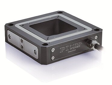
PI’s piezo flexure stages combine sub-nanometer resolution and guiding precision with minimum crosstalk. This makes them particularly suitable for applications in metrology, for super resolution microscopy, for interferometry or in inspection systems for semiconductor chip production. Piezo flexure stages are available for millisecond-settling precision positioning and dynamic scanning with up to several 100 Hertz in up…