

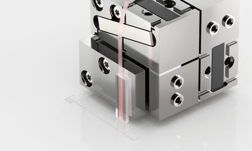
Next-generation devices require wafer-level test solutions capable of validating electrical and optical functions simultaneously in high-volume manufacturing contexts. Our photonic wafer probing technology unifies both domains in a fully automated workflow, combining nanometer-level optical alignment with high-density electrical probing within a compact, ATE-compatible architecture. Miniaturized photonic alignment engines with precise actuation and advanced algorithms ensure stable optical coupling while sustaining production throughput. This approach reduces the cost of test through parallel workflows and offers a scalable path to high-volume manufacturing of electronic photonic integrated circuits (EPICs). Read more