
Dust: 0 particles. Something many of us can only dream of.

At home, dust always comes back. In our flow cabinets it does not get the chance. A flow cabinet blows filtered air over the work surface in one steady direction, so dust and other particles are carried away from the product. Our Fluke 985 particle counter measured 0 particles from 0.3 µm up. That is…
Schaal moeiteloos op van R&D naar serieproductie met de RenAM 500 Flex

Het open-loop poedersysteem maakt het snel en eenvoudig om van poeder te wisselen, waardoor de RenAM 500 Flex bij uitstek geschikt is voor onderzoek en ontwikkeling. Lees meer [Foto uit video van Renishaw Benelux B.V. op linkedin.com]
The Motion Controller — More Than a Command Generator

In Part #3, I wrote about what turns individual precision components into one integrated motion system. An essential part of that system is the motion controller. But what does a motion controller actually do? At first glance, its role seems straightforward: execute commands and move the axes to their required positions. In reality, there is…
Digital vacuum gauges measure better than analog ones. Right?
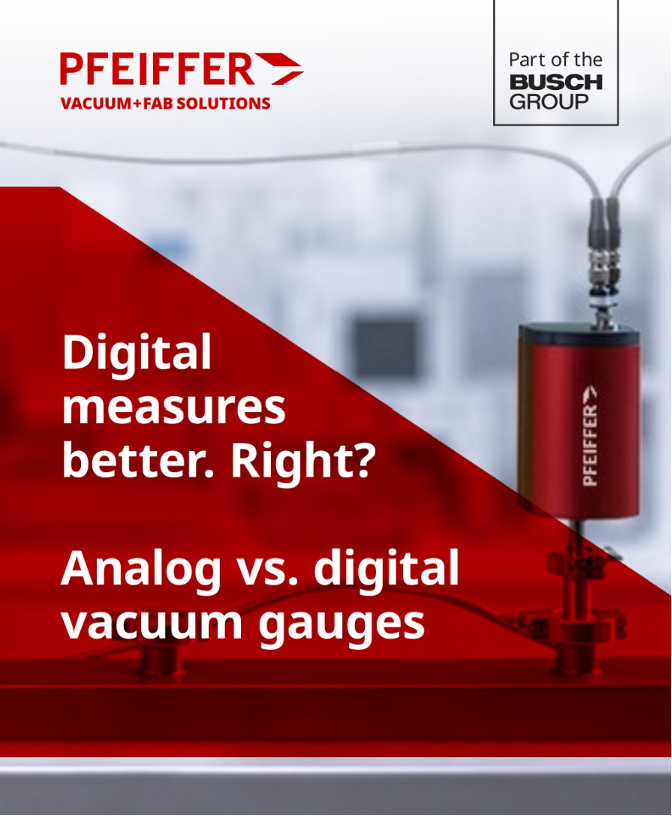
It sounds logical. Newer communication technology, more functionality, more data. Surely the measurement improves, too? Not necessarily. Read more [Picture source: Pfeiffer Vacuum+Fab Solutions on linkedin.com]
Inline wafer scanning
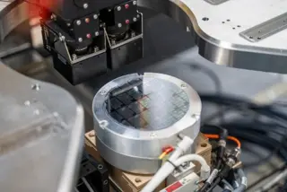
Reliable wafer inspection requires more than high-resolution imaging. Scan speed, image quality and accurate positioning all play an important role in photonic wafer manufacturing. Working alongside IMS, LioniX International and Settels Savenije, Nobleo has contributed to the development and validation of an inline wafer scanning solution that combines high-magnification optical inspection with…
Automated sealant application in aerospace manufacturing with 3D machine vision

How can sealants be applied accurately and consistently to large components with complex geometries? French robotics specialist AKEOPLUS has developed an automated robotic cell that replaces a previously manual process in aerospace manufacturing. Using MVTec HALCON machine vision software, the system determines the actual position and orientation of the components and adjusts the robot’s movements…
Absoluut wegmeetsysteem APM
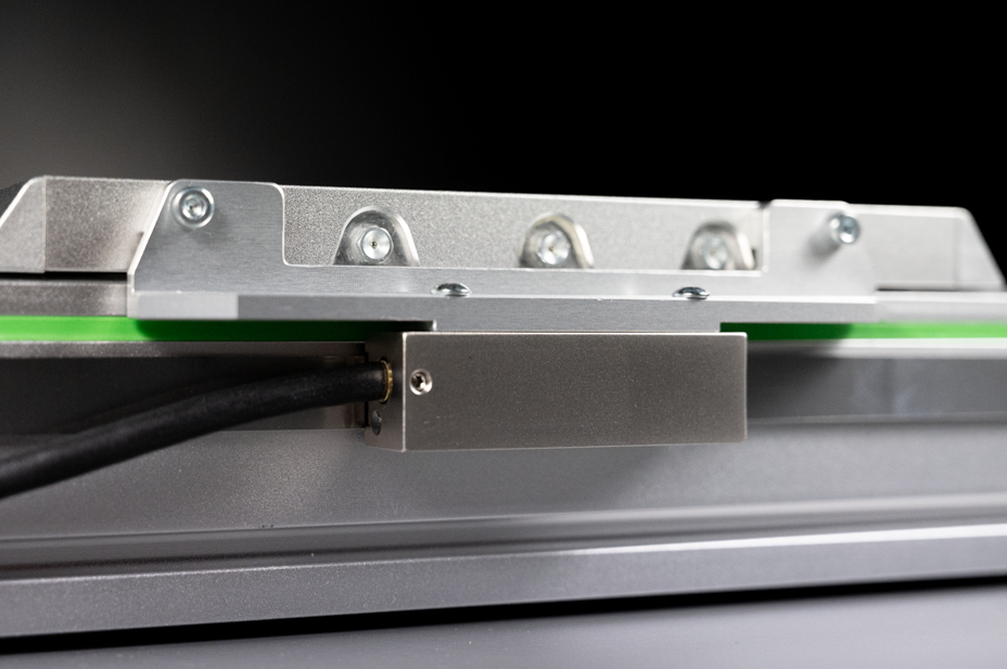
Met het nieuwe absolute wegmeetsysteem APM breiden we ons assortiment voor nauwkeurige lineaire assen uit met nog een belangrijk onderdeel voor complete positioneringsoplossingen uit één hand. In combinatie met onze lineaire assen is het meetsysteem beschikbaar als volledig geïntegreerde oplossing. Dit vereenvoudigt het ontwerp en de inbedrijfstelling, vermindert het aantal interfaces en maakt een nauwkeurige…
Are your CMMs trying to tell you something?

In case you missed it, our Introduction to APOLLO webinar is now available on demand. Find out how predictive condition monitoring helps quality and maintenance teams understand CMM health, spot potential issues earlier, and plan maintenance with more confidence. Read more [Picture source: Hexagon Manufacturing Intelligence on linkedin.com]
Ontdek productieoplossingen waarin snelheid, nauwkeurigheid en gebruiksgemak samenkomen.

Met vTNC7 programmeert u NC-programma’s voor enkelstuks, kleine series en 2,5D-bewerkingen sneller en eenvoudiger. Automatische programmageneratie op basis van 3D-modellen, uitgebreide simulatie én AI-ondersteuning helpen fouten te verminderen en productiviteit te verhogen. Lees meer [Bron foto: HEIDENHAIN Netherlands op linkedin.com]
Trenchless renovation
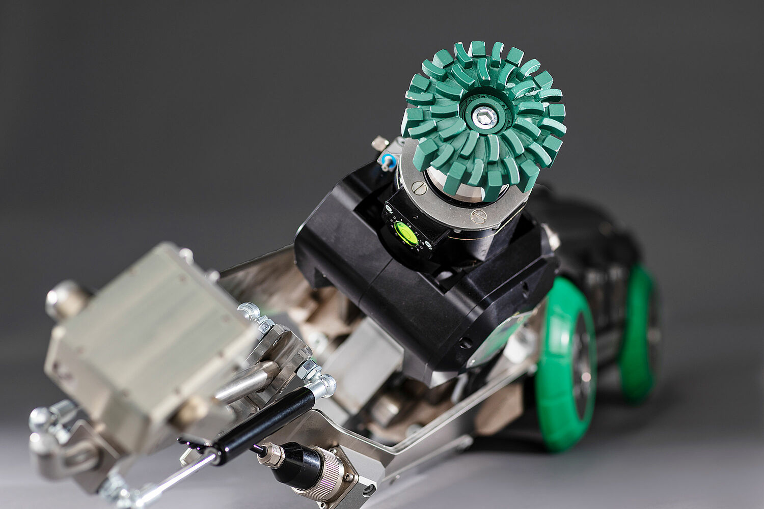
As is the case with any type of infrastructure, sewers require regular maintenance. But the often narrow pipes below the ground are difficult to access. Instead of unearthing them at great expense, users of trenchless renovation procedures use specialized robots that carry out the work in the interior of the pipelines. Pipetronics is a market…