Miniature Bi-Phase Stick-Slip Piezo Nanopositioning Stages – BIX by PI
PI’s new B-421 BIX miniature piezo stages are high-precision nanopositioning systems engineered for applications requiring reliable, accurate linear motion in an extremely small footprint. Built with integrated linear encoders and innovative dual-phase piezo inertia motors, BIX…
Reliable Positioning in 24/7 Industrial Use
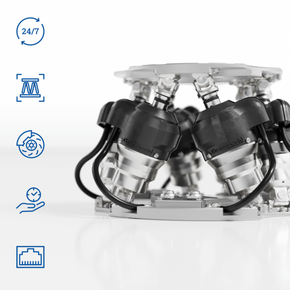
In automated manufacturing processes, unstable positioning, increasing cycle requirements, and impaired system performance lead to quality losses and downtime. Especially under continuous load and at high cycle frequencies, thermal effects, mechanical wear, and a lack of reproducibility reduce process stability, leading to tolerance deviations. The H-815 Industrial Hexapod is specially designed for precise continuous operation and…
PINovAlign6 6-DOF High-Speed Photonics Alignment System – Pivot Point Demo
The Heart of the Customer Application

With longstanding experience and technical know-how, piezo experts from PI produce the perfect functional core piece for customer-specific applications. Piezo actuators perform high-precision movements, piezo elements generate and detect the slightest vibrations. We bring your application to life. Read more
Superresolution Microscopy
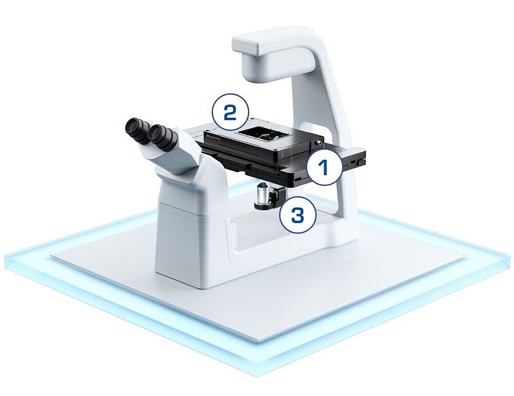
Superresolution microscopy requires precise, reliable, and reproducible sample positioning, objective alignment, and imaging system integration. With its advanced piezo-driven technology, PI’s ultrasound-based microscope platform offers exceptional precision, making it the perfect choice for demanding tasks in modern microscopy. Read more
The Fast Lane to a Precision Advantage

In almost all industrial manufacturing processes, the correct positioning of individual components and their precise alignment to each other are essential for proper product function and manufacturing efficiency. This is even more important as products and their components get smaller and smaller. This ongoing process of miniaturization makes alignment more challenging and more expensive. With 50…
The New Dimension of Precision Automation

Throughput, precision, availability, reliability, and yield – the variety of technologies, the long-term experience in precision positioning, and a modular approach make it possible for PI to react in an application-specific manner to requirements in order to support system integrators and OEMs worldwide in reaching the requested process and machine performances. Read…
Motion Solutions to Increase Throughput in the Photonics Industry – Shown at Photonics West 2025
The demand for photonic integrated circuits (PICs) is growing, everyone is talking about satellite-based internet, and AI is driving the need for increasingly high-performance computer chips. PI offers solutions to help…
Precision Motion Solutions to Help Ramp up Production of Photonics Components
Flexible, Granite-Based Motion Solutions for Precision Automation and Test and Metrology
The X-417 multi-axis system is specifically designed to meet the rigorous demands of industries requiring high dynamics and precision, making it ideal for applications such as testing, metrology, precision automation, and laser processing. Its modular…